Why do we need controlled impedances on PCB?
As circuit design becomes increasingly complex and high-speed, how to ensure the integrity of various signals (especially high-speed signals), that is, to ensure signal quality, has become a problem.
The importance of controlled impedance in a printed circuit board can depend on many variables, including the PCB unique characteristics and how the board will be used.
At this point, will take advantage of transmission line theory to analyze. Control signal characteristic impedance matching becomes the key point. Non-strict impedance control will cause considerable signal reflections and signal distortions, leading to design failures.
To make sure the quality of the signal in complex design, we need to control the resistance and reactance of an electrical circuit.
Such as single-ended impedance 50 ohm ±10%, differential impedance 100ohm ±10%.
The impedance of a PCB is largely determined by the following parameters:
- The distance of the signal layer and potential
- Conductor geometry
- Trackwidth
- Copper thickness
- Permittivity εr
When to use controlled impedance?
We need to use these products in manufacturing, usage, and scenarios. Common signals such as PCI bus, PCI-E bus, USB, Ethernet, DDR memory, LVDS signals, etc., all require impedance control. Impedance control ultimately needs to be realized through PCB design, and higher requirements for PCB board technology. What is the controlled impedance?
Impedance is the sum of the resistance and reactance of an electrical circuit expressed in Ohms. The resistance is the opposition to current flow present in all materials. The reactance is the opposition to current flow resulting from the effect of the inherent capacitance and inductance of the conductor interacting with changes in voltage and current.
In DC circuits there is no reactance and the resistance of copper conductors is typically insignificant. However, in high-speed AC circuits (those with sharp changes in voltage and/or current) the reactance and thus the impedance can become very significant. This can become critical to a design's functionality because of the effects that changes in the impedance along the signals path from the transmitter to receiver will have on the efficiency of power transfer as well as signal integrity.
While a circuit`s speed is often expressed as the frequency of the waveform: the critical concern is the speed at which the voltage and/or current is required to change.
In the process of PCB design and manufacturing, it is necessary to consider Controlled Dielectric
The typical design considerations involved in the determination of the requirement for controlling the impedance are the strength of the signals involved, the susceptibility of the circuit to noise and signal distortion, the criticality of signal timing and the speed at which the signal`s source is attempting to force a change in voltage and/or current.
The design considerations for setting the value of the impedance for the conductor is typically the output impedance of the transmitter and the input impedance of the receiver. The impedance of other conductors (i.e. coaxial cables) in the circuit path will also need to be considered.
The acceptable range (tolerance) for the impedance will need to be determined and taken into account during the design phase as well as when specifying the PCB parameters.
In many cases merely by using software models to determine the anticipated impedance with particular dielectric materials and spacing, followed by requesting these parameters be followed when the PCB`s are fabricated will suffice. This is what we call [controlled dielectric".
For more critical applications you will need to specify [controlled impedance" and supply the actual impedance requirements for the conductors and we will fine-tune the dielectrics and conductors to meet these requirements. The impedance requirements will have to be specified based on the layer and the conductor widths.
PCB Impedance Control calculator
JHY PCB uses the industry standard Polar Impedance Calculator SI8000 to calculate impedance. We provide an impedance report. Typically, designers use published prepreg values from the datasheet to calculate impedance. We have done extensive research over the years to find our "out or press" prepreg thickness, also known as the squeeze-out thickness.
Using these values help us refine our impedance calculations so they are closer to actual values on the finished PCB. This is why we encourage you to work with our team and experienced Field Application Engineers at the conceptual level so that we can help you refine your impedance calculations.


Manufacturing and test Controlled Impedance PCB.
As the operating speed of electronic circuits has increased, so has the need for PCBs to have controlled impedances and the majority of PCB manufacturers are producing them. if the value of controlled impedance is incorrect, it can be very difficult to identify the problem once the PCB is assembled.
Since the impedance depends on many parameters (trace width, trace thickness, laminate thickness, etc.) the majority of PCBs are currently 100% tested for controlled impedance. However, the testing is not normally performed on the actual PCB but on a test coupon manufactured at the same time and on the same panel as the PCB. Sometimes the test coupon is integrated into the main PCB.
Generally, 3 levels of service are available for an impedance control printed circuit board
No impedance control. The impedance tolerance is loose enough that simply making a design with no extra precautions will result in the correct impedance as long as the design is made correctly within the standard specifications. This is the fastest and least expensive option since it places no extra burden on the circuit board manufacturer.
Impedance watching. The designer indicates the impedance control trace. The PCB provider adjusts the (W)width of the trace and (H)height of the dielectric and gets approval on the proposed specifications before starting manufacturing. A TDR (Time Domain Reflectometry) test can be performed to confirm the impedance for an additional cost.
Impedance control. Usually reserved for high-end designs containing either an odd design that doesn't fit the usual microstrip configuration or a tight tolerance. With manufacturing capability limits approaching the dimension requirements, confidence is not high the target impedance will be achieved on the first pass. The circuit board manufacturer first makes the board, getting as close to the target impedance as possible. Next a TDR test is done to determine if the impedance is within specification and adjustments are made as necessary. In the example below, the prepreg (composite fibers "pre-impregnated" with an epoxy) can be added or removed in 1 mil increments to affect H, and changes can also be made to W. Multiple iterations may be needed depending on the design.
In the case of a microstrip, the impedance will depend on 4 parameters:
- H is the height of the dielectric. It can be changed in steps. In this example +/- 1 mil results in +/- 2 ohms
- Er is the dielectric of the material. It is fixed once the material is chosen. Having a good idea of the Er is necessary since +/- 0.1 results in +/- 0.5 Ohms. To make things more complicated, only certain specialty materials like Rogers 4003 have well-defined dielectrics.
- T is the trace thickness. An outer trace is plated, providing a 20% uncertainty in exterior traces. This results in a small uncertainty of +/-0.2 ohms.
- W is the trace width. Typical trace width uncertainty is +/-2 mil which results in an uncertainty of +/- 2 ohms.
50 ohm controlled impedance
In the example provided, if the target impedance is 50 ohm, a 26 mil trace width is required. Since there is a tolerance on the input parameters it translates into a tolerance on the trace width. Achieving the calculated trace size should result in the required impedance.
controlled impedance PCB fabrication notes
Please clearly inform us of the controlled impedance PCB fabrication notes when placing an order for manufacture of PCB.

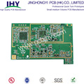
| Type | Impedance Control PCB |
| Layers | 6L |
| Base Material | FR4 Tg170 |
| Dielectric | Prepreg |
| Board Thickness | 1.5mm±10% |
| Copper Weight | 1oz |
| Surface Finish | ENIG 1U" |
| Minimum trace Width/Spacing | 0.1/0.1mm(4/4mils) |
| Solder Mask Color | Green |
| Silkscreen Color | White |
| Min. Hole Size | 0.1mm |
| Min.BGA Pad | 0.25mm |
| Hole Copper Wall Thickness | 25.4um |
| Controlled Impedance | Yes |
| IPC Class III | Yes |
| Flame Retardant Properties | 94 V-0 |
| Application | Military avionics |
Why choose us?
- Save money&time! Achieve peace of mind!
- A professional and trustworthy PCB prototype manufacturer.
- Fastest PCB Prototype.
- One stop solution for various PCB&SMT Stencil.
- Low cost for simple PCB.
- Affordable price for high-tech PCB.
- Minimum orders 1pcs.
- 24-hour online customer service.
- Professional PCB engineer for one-to-one service.
- Shipment on time.
- Guarantee good service and quality from PCB quotation to delivery.
Contact us if you need more details on Cheap 6 Layer PCB. We are ready to answer your questions on packaging, logistics, certification or any other aspects about 50 Ohm Controlled Impedance、Impedance Control Flex PCB. If these products fail to match your need, please contact us and we would like to provide relevant information.
Product Categories : Impedance Control PCB